
-
1371 Old Oakland Rd. San Jose,
CA, 95112 -
(408) 943-8760sales@networkpcb.com

PCB fabrication capabilities have advanced over the years, enabling the production of smaller, more complex, and high-performance boards. These advancements include the ability to create boards with higher layer counts, finer trace widths and spacing, controlled impedance for signal integrity, and various surface finishes to meet specific application requirements. PCB fabrication plays a crucial role in the electronics industry, providing the foundation for the development of a wide range of electronic devices, from consumer electronics to aerospace systems. The success of a product often relies on the quality and reliability of the fabricated PCB, making it a vital step in the overall manufacturing process.
| Description | Production | Advanced |
|---|---|---|
| Structure | 3+n+3 (9+N+9 MAX) | 10+N+10 |
| Layer Count | 2~42L | 50L |
| Min. Board thickness | 0.005" (+/-10%) | 0.005" (+/-10%)s |
| Max. Board thickness | 0.250" (+/-10%) | 0.280" (+/-8%) |
| BGA Pitch | 10mils (0.25mm) | 7mils (0.175mm) |
| Min.BGA pad/space | 7mils/3mils | 5mils/2mils |
| Description | Production | Advanced |
|---|---|---|
| Prepreg (FR4 1067/1086/2113) | Yes | Yes |
| Prepreg (ceramics Ro4350) | Yes | Yes |
| Laser Drillable Prepreg | Yes | Yes |
| laser Drillable core (FR4, PI, PTFE, ceramics) | Yes | Yes |
| laser Drillable Min.Dielectric thickness | 1.5mils | 1.5mils |
| laser Drillable Max.Dielectric thickness | 5mils | 6mils |
| Description | Production | Advanced |
|---|---|---|
| Min / Max | 2.5mils / 6mils | 2mils / 6mils |
| Min via edge to via edge space | 6mils | 4mils |
| True position Tolerance | +/-1mils | +/-1mils |
| Description | Production | Advanced |
|---|---|---|
| Min. Drilled blind via diameter (as drilled) | 10mils | 8mils |
| Min via edge to via edge space (as drilled) | 8mils | 6mils |
| Description | Production | Advanced |
|---|---|---|
| Blind via aspect ratio (dielectric thickness/ Laser drill hole size) | 0.8 | 1 |
| Blind via plating thickness | 0.3~1mils | 0.3~1mils |
| Capture pad A/R | 2mils | 1.5mils |
| Laser via Fill Material | Epoxy resin/Copper paste | Epoxy resin/Copper paste |
| Blind via aspect ratio (as drilled) (dielectric thickness/ drilling hole size) | 0.5 | 0.5 |
| Blind via plating thickness (as drilled) | 0.5mils | 0.8mils |
| Capture pad A/R (as drilled) | 4mils | 3mils |
| Description | Production | Advanced |
|---|---|---|
|
Yes | Yes |
|
Yes | Yes |
| Description | Production | Advanced |
|---|---|---|
| Max. Finish Board Size | 16"X20" | 18"X26" |
| min. Finish Board Size | 0.2"x0.2" | 0.15"*0.15" |
| Max. Board Thickness | 0.250"(+/-10%) | 0.280"(+/-8%) |
| Min. Board Thickness | 0.016"(+/-10%) For 4L | 0.016"(+/-10%) For 4L |
| Description | Production | Advanced |
|---|---|---|
| Layer Count | 4~42L | 50L |
| Layer to Layer Registration | +/-4mils | +/-3mils |
| Description | Production | Advanced |
|---|---|---|
| Min. Drill Size | 6mils | 5mils |
| Min. Hole to Hole Pitch | 20mils(0.5mm) | 18mils(0.45mm) |
| True position Tolerance | +/-3mils | +/-2mils |
| Slot Diameter Tolerance | +/-3mils | +/-2mils |
| Min gap from PTH to track inner layers | 6mils | 4mils |
| Min gap from PTH to the border of rigid flex | 30mils | 20mils |
| Min. PTH Hole edge to PTH Hole edge space | 10mils | 8mils |
| Description | Production | Advanced |
|---|---|---|
| Max. Aspect Ratio | 6:1 | 8:1 |
| Cu Thickness in Through hole | >1mils | >1mils |
| Plated hole size tolerance | +/-2mils | +/-1.5mils |
| NPTH hole tolerance | +/-2mils | +/-1mils |
| Via in pad Fill Material | Epoxy resin/Copper paste | Epoxy resin/Copper paste |
| Description | Production | Advanced |
|---|---|---|
| Min. Trace/Space | 3mils / 3mils | 2.5mils / 2.5mil |
| Min. pad over drill size | 6mils | 4mils |
| Max. Copper thickness | 1~2 oz | 3 oz |
| Line/ pad to board edge | 6mils | 4mils |
| Min gap from Copper to the border of rigid flex | 15mils | 10mils |
| Line Tolerance | +/-20% | +/-10% |
| Description | Production | Advanced |
|---|---|---|
| HASL | 50-1000u" | 50-1000u" |
| HASL+Selective Hard gold | Yes | Yes |
| OSP | 8-20u" | 8-20u" |
| Selective ENIG+OSP | Yes | Yes |
| ENIG(Nickel/Gold) | 80-200u"/2-9 u" | 250u"/ 10u" |
| Immersion Silver | 6-18u" | 6-18u" |
| Hard Gold for Tab | 10-80u" | 10-18u" |
| Immersion Tin | 30u"min | 30u"min |
| ENEPIG (Ni/Pd/Au) | 125u"/4u"/1u" min | 150u"/8u"/2u" min |
| Soft Gold (Nickel/ Gold) | 200u"/ 20u"min | 200u"/ 20u"min |
| Description | Production | Advanced |
|---|---|---|
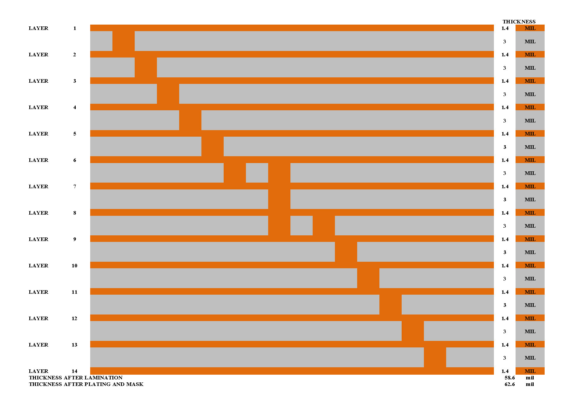
| Thickness(Min) (PI / ADH) | 0.5mils / 1mils | 0.5mils / 1mils |
| dam width | 20mils | 15mils |
| registration tolerance | +/-15mils | +/-10mils |
| Description | Production | Advanced |
|---|---|---|
| S/M Thickness | 0.4mils min | 3mils max |
| Solder dam width | 4mils | 3mils |
| S/M registration tolerance | +/-2.5mils | +/-2mils |
| S/M over line | 3.5mils | 2mils / 2mils |
| Description | Production | Advanced |
|---|---|---|
| Min. Space to SMD pad | 6mils | 4mils |
| Min. Stroke Width | 6mils | 5mils |
| Min. Space to Copper pad | 6mils | 4mils |
| Standard Color | White or Yellow | NA |
| Description | Production | Advanced |
|---|---|---|
| Max. Test Points | 30000 Points | 30000 Points |
| Smallest SMT Pitch | 20mils(0.45mm) | 16mils(0.3mm) |
| Smallest BGA Pitch | 20mils(0.3mm) | 16mils(0.15mm) |
| Description | Production | Advanced |
|---|---|---|
| Min. Rout to copper space | 6mils | 4mils |
| Rout tolerance | +/-2mils | +/-2mils |
| Description | Production | Advanced |
|---|---|---|
| Min. Rout to copper space | 8mils | 4mils |
| Rout tolerance | +/-4mils | +/-3mils |
| Description | Production | Advanced |
|---|---|---|
| Impedance controll | +/-8% | +/-5% |
| Description | Production | Advanced |
|---|---|---|
| PC-5500&PC-5600 | Yes | Yes |
| Description | Production | Advanced |
|---|---|---|
| PI | Yes | Yes |
| FR4 | Yes | Yes |
| Metal | Yes | Yes |
| Description | Production | Advanced |
|---|---|---|
| 3M Type | Yes | Yes |
| Description | Production | Advanced |
|---|---|---|
| Eccobond over Flex width | 60mils | 60mils |
| Description | Production | Advanced |
|---|---|---|
| Min.Trace/Space | 2mils / 2mils | 15mils |
| Min. Copper Thicknesse | 1/3oz | 1/7oz |
| Max. Copper Thickness | 6oz | 10oz |
| Min. Core Thickness | 2mils | 1.5mils |
| Line/ pad to drill hole | 6mils | 4mils |
| Line/ pad to board edge | 8mils | 6mils |
| Line Tolerance | +/-10% | +/-8% |
| Description | Production | Advanced |
|---|---|---|
| Max. Finish Board Size | 19"X24" | 18"X26" |
| min. Finish Board Size | 0.2"x0.2" | 0.15"*0.15" |
| Max. Board Thickness | 0.260"(+/-10%) | 0.280"(+/-8%) |
| Min. Board Thickness | 0.007"(+/-10%) For 4L | 0.005"(+/-10%) For 4L |
| Description | Production | Advanced |
|---|---|---|
| Layer Count | 50L | 60L |
| Layer to Layer Registration | +/-4mils | +/-2mils |
| Description | Production | Advanced |
|---|---|---|
| Min. Drill Size | 6mils | 5mils |
| Min. Hole to Hole Pitch | 18mils(0.5mm) | 14mils(0.45mm) |
| True position Tolerance | +/-3mils | +/-2mils |
| Slot Diameter Tolerance | +/-3mils | +/-2mils |
| Min gap from PTH to track inner layers | 5mils | 4mils |
| Min gap from PTH to the border of rigid flex | 10mils | 8mils |
| Description | Production | Advanced |
|---|---|---|
| Max. Aspect Ratio | 30:1 | 35:1 |
| Cu Thickness in Through hole | 1.5mils | 2oz |
| Plated hole size tolerance | +/-2mils | +/-1.5mils |
| NPTH hole tolerance | +/-2mils | +/-1mils |
| Via in pad Fill Material | Epoxy resin/Copper paste | Epoxy resin/Copper paste |
| Description | Production | Advanced |
|---|---|---|
| Min. Trace/Space | 2.5mils / 2.5mils | 2mils / 2mil |
| Min. pad over drill size | 6mils | 4mils |
| Max. Copper thickness | 10oz | 16oz |
| Line/ pad to board edge | 8mils | 6mils |
| Line Tolerance | +/-15% | +/-8% |
| Description | Production | Advanced |
|---|---|---|
| HASL | 50-1000u" | 50-1000u" |
| HASL+Selective Hard gold | Yes | Yes |
| OSP | 8-20u" | 8-20u" |
| Selective ENIG+OSP | Yes | Yes |
| ENIG(Nickel/Gold) | 80-200u"/2-9 u" | 250u"/ 10u" |
| Immersion Silver | 6-18u" | 6-18u" |
| Hard Gold for Tab | 10-80u" | 10-18u" |
| Immersion Tin | 30u"min | 30u"min |
| ENEPIG (Ni/Pd/Au) | 125u"/4u"/1u" min | 150u"/8u"/2u" min |
| Soft Gold (Nickel/ Gold) | 200u"/ 20u"min | 200u"/ 20u"min |
| Description | Production | Advanced |
|---|---|---|
| S/M Thickness | 0.4mils min | 2mils max |
| Solder dam width | 4mils | 3mils |
| S/M registration tolerance | +/-1.5mils | +/-1mils |
| S/M over line | 3.5mils | 2mils / 2mils |
| Description | Production | Advanced |
|---|---|---|
| Min. Space to SMD pad | 6mils | 4mils |
| Min. Stroke Width | 6mils | 5mils |
| Min. Space to Copper pad | 6mils | 4mils |
| Standard Color | White or Yellow | NA |
| Description | Production | Advanced |
|---|---|---|
| Max. Test Points | 30000 Points | 30000 Points |
| Smallest SMT Pitch | 18mils(0.45mm) | 12mils(0.3mm) |
| Smallest BGA Pitch | 12mils(0.3mm) | 6mils(0.15mm) |
| Description | Production | Advanced |
|---|---|---|
| Min. Rout to copper space | 8mils | 4mils |
| Rout tolerance | +/-4mils | +/-3mils |
| Description | Production | Advanced |
|---|---|---|
| Conductor to center line | 15mils | 15mils |
| X&Y Position Tolerance | +/-4mils | +/-3mils |
| Score Anger | 30o/45o | 30o/45o |
| Score Web | 10mils min | 8mils min |
| Description | Production | Advanced |
|---|---|---|
| bevel anger | 20-71o | 20-71o |
| Bevel Dimensional Tolerance | +/-10mils | +/-10mils |