
- 1371 Old Oakland Rd. San Jose,
CA, 95112 -
(408) 943-8760sales@networkpcb.com
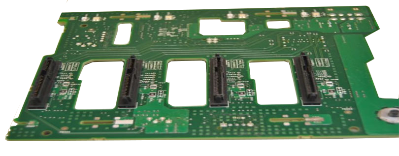
We specialize in producing larger format printed circuit boards that are used as backbones for connecting several PCBs together to ultimately form a computer bus. Typically, they do not contain active components; rather, they serve as a connection centre between active duty PCBs. Our back plane PCBs often incorporate a wide variety of features including blind / buried vias, high-speed / high-signal integrity materials, back drilling, and controlled impedance.
Backplane PCBs form the backbone of a system such as control panels for various industrial, computing, & military use. They provide greater reliability in connecting multiple PCBs due to their static nature, as opposed to cables that need to be flexed every time a card is removed, thereby reducing the life of that component/connection.
We provide services from quick turn prototype through mass PCB production in Backplane board, meeting the customer lead- time to market requirements. We thrive in a high mix, quick turn environment.
| Parameter | Standard | High | Advanced |
|---|---|---|---|
| Layer Count (Max. Layers) | 16 | 40 | 60+ |
| PCB Size (Max.) | 1100 mm × 500 mm | 1200 mm × 550 mm | 1200 mm × 630 mm |
| Thickness (Max.) | 8 mm | 10 mm | 15 mm+ |
| Outer Layer Line Width/Space | 0.006" / 0.006" | 0.005" / 0.005" | 0.004" / 0.004" |
| Press-fit Hole Size Tolerance | +/-2 mil | +/-2 mil | +2 / -1 mil |
| Through Hole Aspect Ratio | 14:01 | 17:01 | 20:01 |
| Drill Registration | +/-5 mil | +/-4 mil | +/-3 mil |
| Buried Vias | Yes | Yes | Yes |
| Blind Vias | Layers n to n-1 | Layers n to n-2 | Layers n to n-3 |